I needed to draw a timing diagram for a mixed signal class I took. I found
The problem I was solving is shown below in the image. It's rather tedious to figure out. You have to remember that once a gate capacitance is charged up it ideally holds that charge until it is connected to again by either Vdd or Ground.
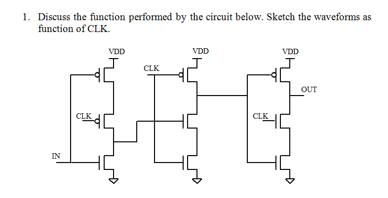

The gate turns out to be a falling edge triggered flip flop. You can see it in the wikipedia:flip flop article that includes this diagram which was found after I did the timing diagram.
0 Comments