Charge Pump Articles – No Inductors Allowed

XFAB Links


XFAB PhotoDiode Cross Sections png

XFAB has integrated photo diodes in the XH018 process.  However it was difficult to find the scaling factor for the light input pin on the photo diode schematic symbol.  The only place I have found it thus far is in the photo diode model:

The photodiode light input is a third terminal on the diode symbol. In order to do a simulation one must know how light intensity scales to light input terminal voltage. This information was discovered in the comments one of the photodiode library files.

Excerpt from file: dphoa.scs

* TERMINALS: anode=PSUB, cathode=DNWELL, lpower=lpower[1uV==1uW] 
* VARIABLES: area[m2], perimeter[m], wavelength[1==1um] 
* TNOM = 27 deg C; TEMP=27 deg C 


Paper Links

Block-Diagram-0p35-Solar-Energy-Scavenger

Solar-Cell-Circuit-Model

A 0.35 um CMOS Solar Energy Scavenger with Power Storage Management System


Cross couple voltage doubler.

Design of Very Low Voltage CMOS Rectifier Circuits  – Bulk connection is very important in voltage multipliers.  In a Dickson charge pump DTMOS connection is the one that works best.  That assumes you are using isolated transistors so you do not end up with elevated theshold voltages.

Dickson model above simulates the action of the main line of the voltage multiplier but does not cover the power required by the clock inverters that drive the 2 phases.  Thus it does not apply for over all efficiency calculations.


The current of the 5V section of the level shifter is too high for very low consumption circuits.  My simulations had it at 10uAmp @ 1MHz.


This charge recycling scheme does not work if the stray capacitance is negligible compared to the pump capacitance. My lack of understanding lead me to try using it with my test design simulations. When no difference in current consumption showed up I had to scatch my head.


Voltage Regulation for Energy Scavenging


Circuit Implementation Notes

  • Area Efficiency Improvment of CMOS Charge Pumps:  If p is the ratio of stray capacitance to desired capacitance (Cp  p Ca) and is determined by the type of capacitors used. For double poly capacitors, this value is usually between 10 and 20 percent. Thin oxide MOS capacitors provide 5-15% stray capacitance, with a higher capacitance per unit area than double poly capacitors. For poly-metal capacitors, p can be as much as 20-50%.

Getting Cadence Mixed Signal Photo Diode Circuit to Compile

The key to solving the problem was carefully looking at the Cadence text output and then opening the correct log file named: ahdlcmi.out .  This file was located in the project folders.

The following problems were flagged

  • /usr/include/gnu/stub-32.h
  • /usr/lib/crti.o
  • ld can not find -lc

ld can not find -lc     was the linker saying it could not find liba.c. 

These were installed using Yast and selecting

  • glibc-devel-static
  • glibc-devel-static-32bit

Both 32 and 64 bit were installed because it was not known which was needed.  I suspect it is the 32 bit version due to the stub-32.h header file that was earlier a problem.


Cadence XKIT PDK Process Design Kit Installation Notes

Conclusions

The problems of phase 1 below were due to running the

xkit -t xh018

script from a directory that already contained entries resulting from another technology.  That confused it well and good.


Phase 1

Research Links

….more

1.2 Volt Band Gap Reference After the Start Up Circuit is fixed

Report Delivered for this project here

This entry records the steps taken after the above report was delivered.

BookSeeBookSee

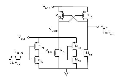
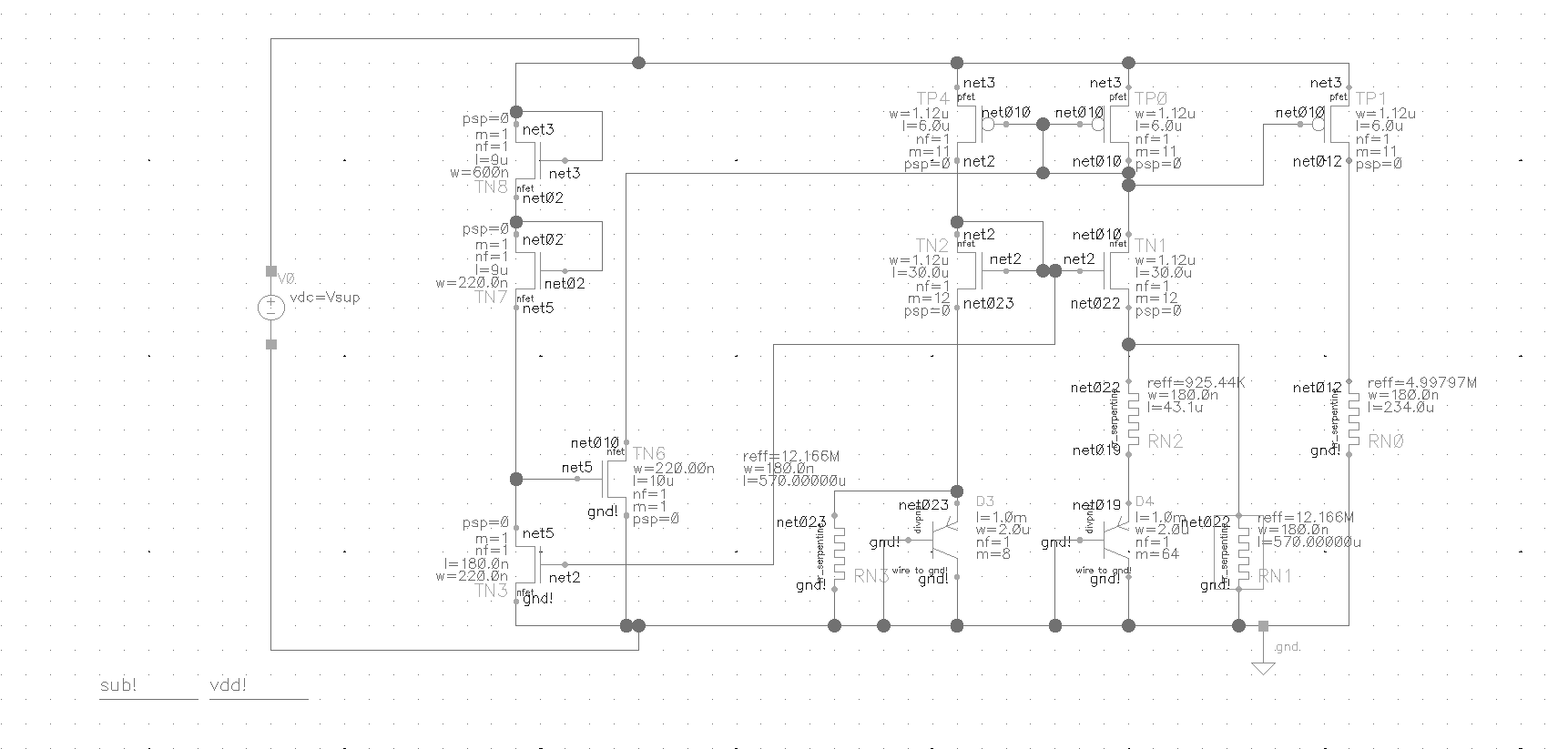
TN3 was too long previous to this fix. Thus TN5 was not shutting off sufficiently and drawing too much current off of the current mirror.

Next Steps:

  • Redo startup transient analysisResearch Links
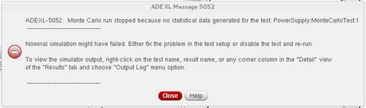
  • Redo Monte Carlo analysis including startup circuit
  • Go over the circuit for any possible reduction in sizes in the diodes and resistors.


Transient Analysis Redo Results

  • 1 to 1.8V supply voltage in 0.1 Volt steps.
  • About 0.5 mSec to turn on

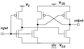
Tweaking Monte Carlo V2 for output concavityResearch Links


Research 0L0inks

Tweaking Monte Carlo V2 for output concavity


Round Two Monte Carlo Results

Research Links

  • 968 in the desired working range
  • 32 versions exhibited in the bins: 47,62,93 mV
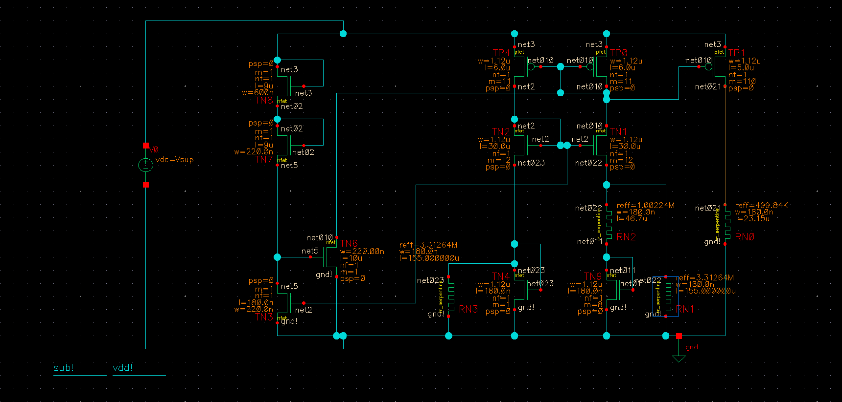
 

Preliminary Layout

  • The big rectangles are the diode connected bjt's
  • The little rectangles are the FETS
  • The long thin red lines are the resistors

FETs as Diodes

  • One way around the huge diodes would be to use nmos fets in weak inversion and diode connected.  Their characteristic is exponential under these circumstances and the worst case threshold voltage is 150mV less than the huge diode drop.  I am not sure if this is practical or not in actual practice but the simulation below looks good.
  • Resistor values had to be altered.  The large resistors can be reduced from around 12 MOhm down to about 3 MOhm.

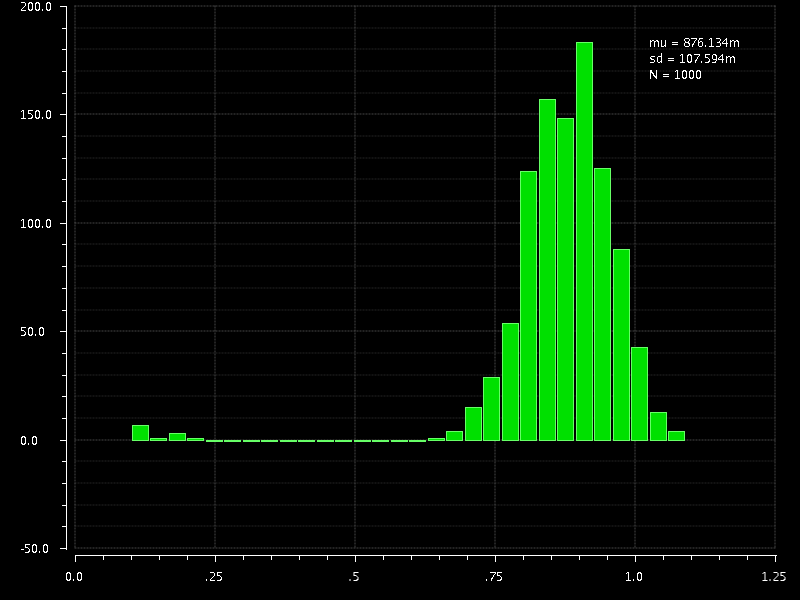
  • The FET mismatch leads to the following Monte Carlo distribution.  Looks like I need to make the "diode" FETs bigger.


DIPDNW in the diode position

  • Appears to be 1/60 the area of the divpnp version

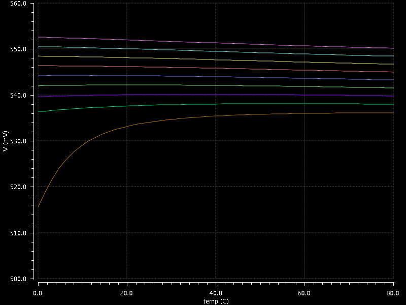
Monte Carlo Analysis @T=27 degrees C shows it well behaved more or less.  Still has issue with startup at times.

Monte Carlo Analysis @T=80 degrees C shows it well behaved.  Distribution at the low end it gone. 


Monte Carlo Analysis @T=0 degrees C shows markedly more false starts than higher temperatures

ac


Importing a Design Library into Cadence Virtuoso

I had a problem where when I returned to my opensuse based machine my Cadence design library was no where to be seen in the library manager.  In order to for it to show up again in the list there are 2 ways of approaching the problem.

  • With the Log window( not sure what it is called ) click: Tools > Library Path Manager
  • or you can directly edit  CDS.lib

I think the first method is the way that is intended by the software authors but who can tell with an interface as bad as Cadence?

Connecting to Cadence Remotely Via SSH on a Linux Box

On a box connected on the same local network   –  ssh -Y -l username IP address

The -Y switch enables trusted forwarding of X Window applications from the host computer so that they can run in the X Window environment of the client computer. The -l switch allows you to specify the user name you want to log in under.

VPN Setup: Ubuntu VPN connection is set up by clicking on the anti parallel UP/DOWN arrows at the top right hand side of the display. Configure the VPN clicking on VPN connections.  When I previously tried finding this via the system tools > network there was no mention of VPN there.  

Settings

  • Use the PPTP protocol
  • Enter the VPN server address
  • User / Password
  • In the advanced settings select SEND PPP ECHO PACKETS.

150.162.11.138