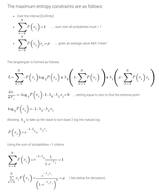
Samsung SGH-I777 Galaxy S2 Battery Notes
![bateria-samsung-galaxy-s2-i9100-eb-l1a2gba-original-frete-gr-15292-MLB20098831015_052014-O[1]](http://www.amarketplaceofideas.com/wp-content/uploads/2014/06/bateria-samsung-galaxy-s2-i9100-eb-l1a2gba-original-frete-gr-15292-MLB20098831015_052014-O1.jpg)
The battery from my cell phone.
I have found that just getting a new battery for my SGH-i777 is not enough. When I put the new battery with slightly different part number in the phone it will not charge. If the phone was on it turns off and the green battery charging animation icon comes up for a bit then it also turns off and then back on / off / on to infinity. Quite an annoying problem and quite obvious there is more than meets the eye here. It could be as simple as Samsung wanting to sell batteries. However given the NSA's involvement in everything communications now days I have to wonder. After a little googling I found the following images in an article about how the near field communications circuitry is in the battery. One has to assume the NSA knows we know to take the battery out of our phones. So what to do? Put a radio in the battery. I have no idea what other "features" are in the battery but I have to assume there are a few.
The weird thing about this is even though I used an external charger to charge the new battery the phone refused to link to the cell phone system with it used to power the phone. This in spite of the fact that the new battery with part number eb-f1a2gbu is called out as a replacement battery for the Galaxy SII.
Whether it is Samsung conspiring to sell more batteries or the NSA forcing some backdoor communications path on the cell phone companies I find the cell phone network to be highly oppressive. It will not be a free media until someone comes up with something subversive.
Research Links
- Why does it say Near Field Communication on the battery?
- MercadoLivre: Eb-l1a2gba original battery that works
- Google: eb-f1a2gbu – replacement battery that does not work


Government
How to Retrieve Mothers Maiden Name for CNPQ.br Registration
When registering on the Curriculo Lattes / Plataforma Lattes if you want to enter your CPF you must have entered your mothers name so that it matches name used when you registered for CPF. If it does not match then you will get the following error when you try to enter your CPF:

So if you get this error like I did then you must find out what form of your mothers name you registered with. Since I did this over 10 years earlier I did not remember. You see Latin America uses all the names First Middle Maiden Married. Well I forgot having used this full form. The solution to this problem is to go here:
- Sistema seguranca digital When you arrive at the page click on Solicitar Accesso.
You can then enter your CPF and it will come back with a form that has your mothers name already filled out. Much convenient because I do not want to go stand in line at some government organ. This is the typical solution in Brazil which I do not find fun in the least.
I managed to get my mothers named fixed and adjust my phone and address. When I tried to modify the blank CPF field I got the following:

Never mind that I did not try 3 times to change my CPF and that I tried only once. FYI: In spite of my name not agreeing exactly with my CPF registration it did not flag that error until my mothers name coincided exactly. Now I have to wait another 3 hours as I left my middle name off of my CNPQ registration.