XFAB Links

XFAB has integrated photo diodes in the XH018 process. However it was difficult to find the scaling factor for the light input pin on the photo diode schematic symbol. The only place I have found it thus far is in the photo diode model:
The photodiode light input is a third terminal on the diode symbol. In order to do a simulation one must know how light intensity scales to light input terminal voltage. This information was discovered in the comments one of the photodiode library files.
Excerpt from file: dphoa.scs
* TERMINALS: anode=PSUB, cathode=DNWELL, lpower=lpower[1uV==1uW]
* VARIABLES: area[m2], perimeter[m], wavelength[1==1um]
* TNOM = 27 deg C; TEMP=27 deg C
Paper Links


A 0.35 um CMOS Solar Energy Scavenger with Power Storage Management System
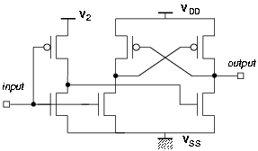
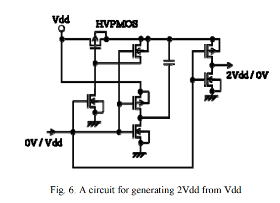
Cross couple voltage doubler.

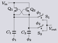
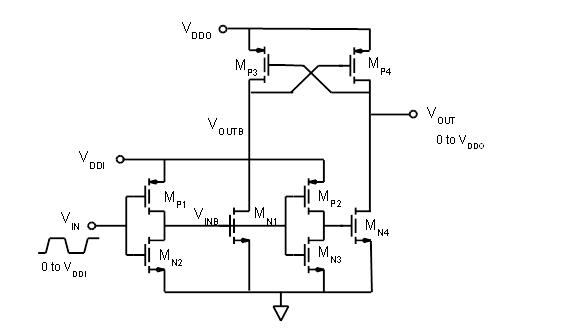
Design of Very Low Voltage CMOS Rectifier Circuits – Bulk connection is very important in voltage multipliers. In a Dickson charge pump DTMOS connection is the one that works best. That assumes you are using isolated transistors so you do not end up with elevated theshold voltages.

Dickson model above simulates the action of the main line of the voltage multiplier but does not cover the power required by the clock inverters that drive the 2 phases. Thus it does not apply for over all efficiency calculations.
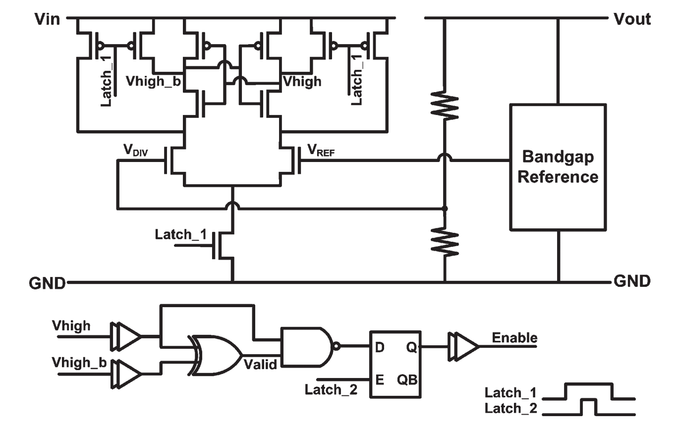
The current of the 5V section of the level shifter is too high for very low consumption circuits. My simulations had it at 10uAmp @ 1MHz.

This charge recycling scheme does not work if the stray capacitance is negligible compared to the pump capacitance. My lack of understanding lead me to try using it with my test design simulations. When no difference in current consumption showed up I had to scatch my head.
Voltage Regulation for Energy Scavenging


Circuit Implementation Notes
-
Area Efficiency Improvment of CMOS Charge Pumps: If p is the ratio of stray capacitance to desired capacitance (Cp � p Ca) and is determined by the type of capacitors used. For double poly capacitors, this value is usually between 10 and 20 percent. Thin oxide MOS capacitors provide 5-15% stray capacitance, with a higher capacitance per unit area than double poly capacitors. For poly-metal capacitors, p can be as much as 20-50%.