Charge Pump Articles – No Inductors Allowed

XFAB Links


XFAB PhotoDiode Cross Sections png

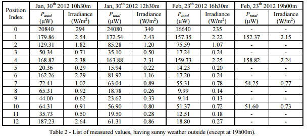
XFAB has integrated photo diodes in the XH018 process.  However it was difficult to find the scaling factor for the light input pin on the photo diode schematic symbol.  The only place I have found it thus far is in the photo diode model:

The photodiode light input is a third terminal on the diode symbol. In order to do a simulation one must know how light intensity scales to light input terminal voltage. This information was discovered in the comments one of the photodiode library files.

Excerpt from file: dphoa.scs

* TERMINALS: anode=PSUB, cathode=DNWELL, lpower=lpower[1uV==1uW] 
* VARIABLES: area[m2], perimeter[m], wavelength[1==1um] 
* TNOM = 27 deg C; TEMP=27 deg C 


Paper Links

Block-Diagram-0p35-Solar-Energy-Scavenger

Solar-Cell-Circuit-Model

A 0.35 um CMOS Solar Energy Scavenger with Power Storage Management System
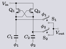


Cross couple voltage doubler.

Design of Very Low Voltage CMOS Rectifier Circuits  – Bulk connection is very important in voltage multipliers.  In a Dickson charge pump DTMOS connection is the one that works best.  That assumes you are using isolated transistors so you do not end up with elevated theshold voltages.

Dickson model above simulates the action of the main line of the voltage multiplier but does not cover the power required by the clock inverters that drive the 2 phases.  Thus it does not apply for over all efficiency calculations.
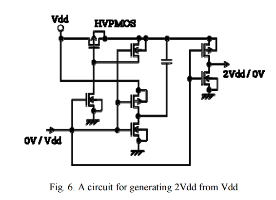
 

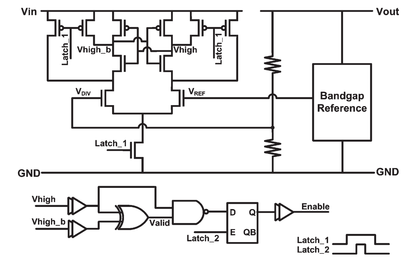
The current of the 5V section of the level shifter is too high for very low consumption circuits.  My simulations had it at 10uAmp @ 1MHz.
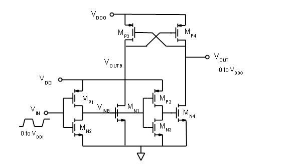
 

This charge recycling scheme does not work if the stray capacitance is negligible compared to the pump capacitance. My lack of understanding lead me to try using it with my test design simulations. When no difference in current consumption showed up I had to scatch my head.


Voltage Regulation for Energy Scavenging


Circuit Implementation Notes

  • Area Efficiency Improvment of CMOS Charge Pumps:  If p is the ratio of stray capacitance to desired capacitance (Cp  p Ca) and is determined by the type of capacitors used. For double poly capacitors, this value is usually between 10 and 20 percent. Thin oxide MOS capacitors provide 5-15% stray capacitance, with a higher capacitance per unit area than double poly capacitors. For poly-metal capacitors, p can be as much as 20-50%.

CI Brasil – CT1 Porto Alegre Inscription Open

Calendário CT1

  • 17/04/14         Início da Fase 1 – Abertura das inscrições
  • 22/06/14         Fim da Fase 1 – Fechamento das inscrições. 
  • 26/06/14         Início da Fase 2 – Prova online
  • 04/07/14         Fim da Fase 2 – Divulgação dos selecionados
  • 04/07/14         Início da Fase 3 – Início do envio de documentos
  • 18/07/14         Fim da Fase 3 – Último dia para envio da documentação POR SEDEX (data de postagem).
  • 12/07/14         Divulgação de vagas remanescentes
  • 04/08/13         Matrícula presencial
  • 05/08/14         Cerimônia de Abertura e Orientation Day (manhã)………..Início do Programa de Formação (tarde).
  • 31/07/15         Fim do Programa de Formação

Other Options for Studying IC Design in Brazil

Return to Mother Page: Studying IC Design in Brazil

IC related entities in Brazil – Many appear to be supported by the government

Other Industry Entry Points in Brazil

University with IC programs – This is an alternative to the CT1, CT2 programs if the only way in is a competition with engineering talent with 80 vacancies per year in a country of 240 million people.

UFSC – The RF IC program is headed by Fernando Rangel de Sousa – My Summary Page

UFSC – The RF IC program is headed by Fernando Rangel de Sousa – My Summary Page

PPGEEL Page with LCI outgoing links

Return to Mother Page: Studying IC Design in Brazil

Research Links


The Cadence software is used on the following courses:

  • Undergraduate courses

    • EEL7303 – Analog Circuits
    •  EEL7411 – RF Circuits
  • Graduate courses

    •  EEL6712 – Introduction to IC Design
    •  EEL6713 – Analog IC Design
    • EEL6750 – RF Electronic Circuits

2013/3 – DisciplinasHorários

2013/2 – DisciplinasHorários

2013/1 – Disciplinas, Horários

From: Horários das disciplinas

Classes 2014 Trimester 1 starting March 10

Fernando Rangel de Sousa – head of the RF IC program at UFSC

Fernando Rangel is said to use ADS much and Cadence much less.  This may defeat my objectives.


Possible References


Application Form


Calendar  Primeiro Trimestre

  • Data limite para inscrição:  30 de Novembro
  • Resultado da seleção: a partir de 23 de Dezembro

Selection Results

CTI Renato Archer – Brazilian government funded university for IC design

CTI Renato Archer – Brazilian government funded university for IC design 

It's basically "Cadence University" that you pay 30k for in the USA.

Return to Mother Page: Studying IC Design in Brazil


Calendário CT2/CT3

The following cut and paste from the calendar should only be used as a guide.  It can change.  Appears the test date may be changed but that may be in error. USE THE GIGANTIC LINK ABOVE FOR CRITICAL PATH ITEMS.

Calendário CT2/CT3

12/11/13         Início do período de inscrições.
12/01/14         Fim do período de inscrições. [PRORROGADA ATÉ O DIA 27/01]
30 e 31/01/14         Prova online de seleção
07/02/14         Divulgação dos selecionados da 1ª Chamada. Os candidatos selecionados receberão um e-mail solicitando a confirmação de participação e o envio de documentação complementar escaneada.
06/03/14         Matricula Presencial, apresentação de documentos oficiais e orientações.
10/03/14          Início do Curso
28/02/15         Fim do Curso.


Summary: The Brazilian push into ICs seems to be to use the Cadence design classes in a 1 year program.

Research Links


CI Initiative – The CT1 and CT2 programs look to be little more than Cadence training programs augmented by an internship afterwards


…. more